DESIGN AND FABRICATION OF PHOTONIC STRUCTURES USING FOCUSED ION BEAM TECHNOLOGY
In the era of rapid technological development of integrated photonics and the associated high demand for modern and efficient ways of fabricating structures, we address these problems by making available an optimal process for fabricating photonic structures using a focused ion beam.
Nanores, a nanotechnology laboratory, has advanced dual-beam SEM/FIB microscopy systems in its laboratory base that enable both materials research and prototyping at the micro and nano scale. The company specializes in using focused ion beam technology to fabricate photonic structures of various types for so-called integrated photonics applications. Two different DualBeam systems are available, differing in the source of the ion beam: Ga-FIB (Gallium Focused Ion Beam), Xe-PFIB (Xenon Plasma Focused Ion Beam). The ion beam is selected according to the application and its choice depends on the material you are working with and the structure you want to make. This is due, among other things, to the different operating parameters of these beams, such as, for example, the current range and the beam spot width depending on the accelerating voltage. In addition, a great deal depends on the physics of the interaction of the beam with the substrate.
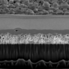
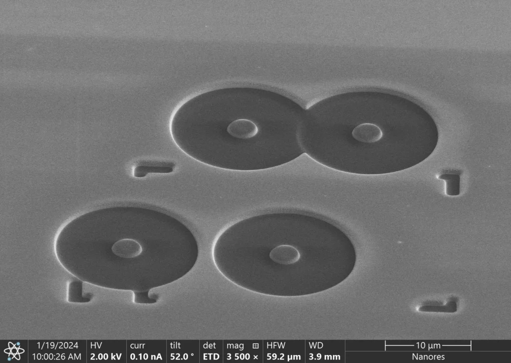
We have experience in the design and prototyping of micro-pillar and mesa structures in Group III-V semiconductor materials such as GaAs and InP with InGaAs/GaAs and InAs/InP quantum dots, respectively. We can fabricate single structures as well as entire series, depending on the scope of work and demand in the experiment.
As part of structure design, we are able to perform FDTD numerical simulations to determine optimal structure dimensions and optimize photon emission collection, as well as perform spectroscopic studies of fabricated structures, such as: micro-photoluminescence, photon correlation.
In addition, in our laboratory it is possible to apply layers of various elements, e.g. Au, Ag, Pt, C using a sputtering machine or a gas injection system (GIS). If necessary, we are able to use external apparatus to modify surfaces with wet etching. Thanks to the DualBeam SEM/FIB system software and yes streamfiles (instructions describing the dynamics of the ion beam, its trajectories, operating parameters), we are able to make any shape and size of structures.
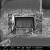
In addition, we have experience in fabricating structures such as photonic crystals and Fresnel lenses. We can perform sample surface mapping by using a marker array as a reference system to locate actively optical objects, such as quantum dots. The cost of fabrication of the structure depends on many factors, so the pricing along with the scope of the project is always determined individually depending on the customer’s needs.